Odyssey Semiconductor Technologies, Inc.
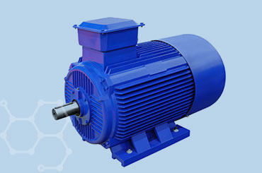
A power semiconductor company using Gallium Nitride to create breakthrough technology for high performance and high volume power applications

Odyssey Semiconductor was founded by Rick Brown and James R. Shealy. Our disruptive proprietary technology will enable gallium nitride (GaN) to displace silicon carbide (SiC) as the emerging high-voltage power-switching semiconductor material of choice.

Innovating the Future

We believe the GaN is the future of high-voltage transistors. The material properties of GaN make it a far superior option over silicon carbide (SiC) for high-voltage power-switching applications. However, GaN processing technology has not produced a viable GaN high voltage switching transistor operating above 1,000 V. Current devices are largely horizontal conduction devices based on radio frequency (RF) designs modified to operate at high voltage. These designs are not scalable beyond 1,000 V for operating voltage, which limits their use to low-voltage consumer electronics applications.

Odyssey Semiconductor’s unique GaN processing technology allows for the realization of vertical current conduction GaN devices which extends application voltages from 1,000 V to over 10,000 V, allowing GaN power switching devices to extend well beyond the consumer electronics application space and into more demanding applications such as electric vehicles, industrial motor control, and energy grid applications.

Focus Industries

Industrial Motors

With over 40% of global energy consumed by electric motors, there is a pressing need for more efficient and smaller power circuits. Vertical GaN enables designers to meet these needs.
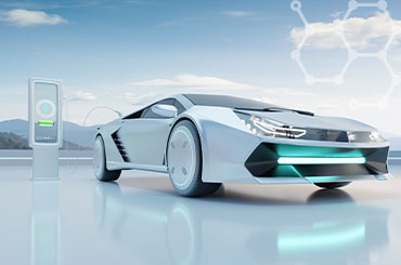
Electric Vehicles

To expand the adoption of electric vehicles, there is a need to extend range while also reducing total solution cost. Silicon FETs do not provide enough efficiency and silicon carbide FETs are too expensive. Vertical GaN is the answer.

Renewable Energy

Generating and distributing energy from renewable sources has created new applications for power conversion. The need to operate at high-voltages and high efficiency presents unique challenges that vertical GaN is best to solve.

Our Headquarters

Odyssey Semiconductor’s global headquarters supports R&D, wafer fabrication and corporate functions. Located in Ithaca, NY, the 10,000 sqft facility includes multiple cleanrooms with photolithography and other semiconductor manufacturing process equipment, an advanced metrology lab and a power applications lab. Additional spaces for R&D and corporate functions are also included. The facility is optimally designed to support all aspects of vertical GaN power switch development and fabrication.
Additionally, Odyssey uses the facility to offer a unique breadth of semiconductor foundry services by filling the gap between university and large-scale wafer foundries. In addition to GaN, our foundry is capable of designing and optimizing processes in many compound semiconductor materials and substrate dimensions.

Our Team

Odyssey Semiconductor’s management team and board of directors consist of highly respected professionals in the semiconductor industry and academia. The management team alone has over 90 years of combined experience in the industry.